PoE32 Lite
On this page
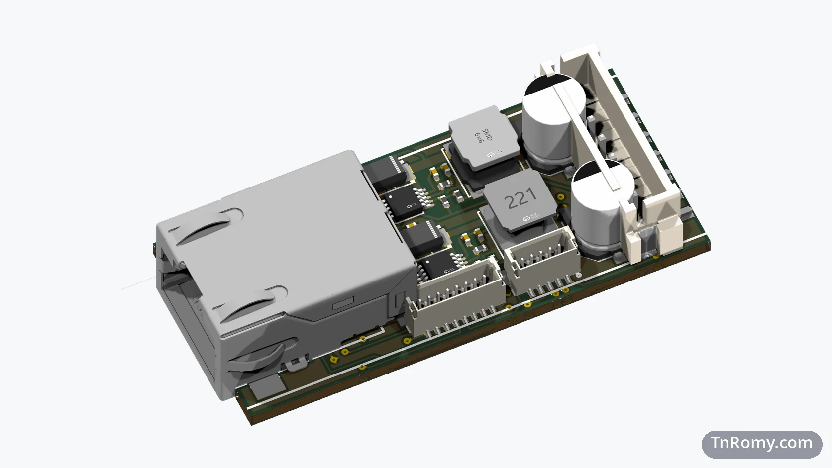
PoE32 Lite is a small microcontroller board that takes both its data and its power from a single Ethernet cable. It is called Lite because its chip, the CH32V203, supports Ethernet at 10 Mbit/s only; a later board built on another chip will do Fast Ethernet, 100 Mbit/s. A RISC-V chip with Ethernet built in, a Power over Ethernet front end, and two supply rails fit on a board of 50 × 23 mm that slides into an off-the-shelf aluminium enclosure, with printed circuit boards in place of the enclosure's end caps.
It is the base of a small family. The board carries the microcontroller, the network, and the power; whatever a particular device has to do lives on a separate module that doubles as the enclosure's rear cover. This page is about the third revision, v3: the first one with the whole PoE power path on the board. The two revisions before it have their own pages.
At a glance
| Board | PoE32 Lite, the base board of the PoE32 family |
|---|---|
| Revision | v3, ordered in December 2025 |
| MCU | WCH CH32V203RBT6, RISC-V, with the Ethernet MAC and a 10BASE-T PHY on the chip |
| Size | 50 × 23 mm, 1.6 mm thick |
| Power | Power over Ethernet, IEEE 802.3af powered device; 24 V and 3.3 V rails on the board |
| Interfaces | Ethernet (RJ45 with integrated magnetics), I²C, SWD and UART for debugging, a 7-pin module header with SPI, ADC, PWM, and 24 V |
| PCB | 4 layers, components on both sides |
| Enclosure | Extruded aluminium profile, about 25 × 25 mm in cross-section and 50 mm long, with PCB end caps |
| Status | Prototype: v3 runs with jumper wires, v4 is being designed |
| Files | 3D model (STEP) attached below; component values and the bill of materials are not published |
Why it exists
The board most people reach for in a small connected device today is an ESP32, and it talks over WiFi. But the word wireless in WiFi only describes the data. The power still arrives over a wire, unless the device runs on a battery, and a battery runs out sooner or later. So in practice one cable ends up plugged into the board anyway. If there is going to be one cable regardless, I would rather it be an Ethernet cable: with Power over Ethernet, that single cable carries the data and the power together.
Most of these devices also never move. A sensor on a wall, a controller in a panel, a node of a fire alarm: they stay where they were installed for years. Mobility is the one thing WiFi gives that a cable cannot, and a stationary device does not need it. What a stationary device does need is a link that stays up, and a cable is more stable than radio.
Speed is not a reason to avoid a cable either. Ten megabits per second is plenty for telemetry and MQTT, which is what these devices exchange. And there is security. A WiFi device can be reached by anyone within radio range, so its attack surface extends past the walls of the building. A device on a cable can only be reached by someone who has, at the very least, physical access to the same network.
The size follows from where such a board ends up: tucked behind a ceiling, inside a junction box, next to a detector. So it has to be as small as I can make it, and it has no DC jack at all. Power comes only from the Ethernet port. When a device has to run from a separate supply, a PoE injector does the job, and the power still arrives over the Ethernet cable.
The same size is also why the board stops at IEEE 802.3af, the lowest power class of the standard. Moving up to 802.3at would need a much larger flyback transformer, because one of the rails is 24 V. If the board only had to produce 3.3 V, the picture would be different, but at 50 × 23 mm with a 24 V output, 802.3af is what fits.
What v1 and v2 lacked
v1 put everything on one board, including the fire alarm drivers, and had no Ethernet port of its own. v2 fixed both: the fire alarm circuit moved out to the enclosure's rear cover, and a low-profile RJ45 came onto the board. But v2 still took its power from a separate PoE module on a cable, and the arrangement inside the enclosure was far from ideal. v3 exists to bring the power onto the board.
What v3 is
v3 is the first revision with the whole PoE power path on the main board, and nearly everything about it follows from that. I replaced the RJ45 with one that has the magnetics built in, so the separate transformer disappeared. Behind it come two diode bridges, a surge suppressor, a PD controller, and two buck converters, one for 24 V and one for 3.3 V.
There was not enough area for all of that on one side, so the board uses both. The tall power parts, the inductors and the electrolytic capacitors, sit on top with the connectors. The flat parts, the microcontroller and the PD controller, sit underneath. Inside a profile only 25 mm tall, this uses both halves of the space instead of one.
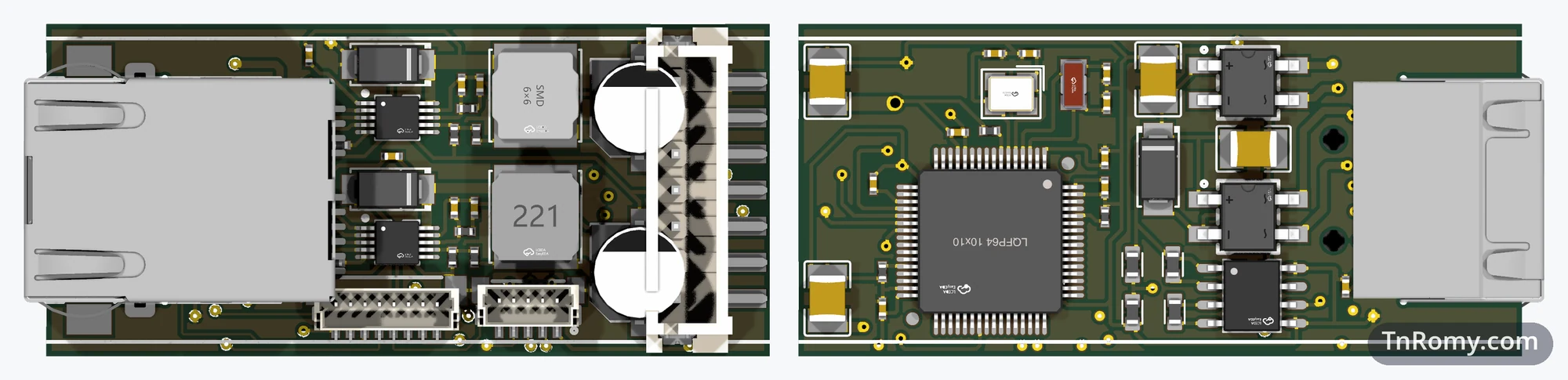
Routing it was the densest work of the three revisions. Halfway through the layout, I added inner copper layers, and the board ended up with four. Over the following five days the layout went through about thirty-five iterations before I ordered it on 17 December, assembled, ten boards.
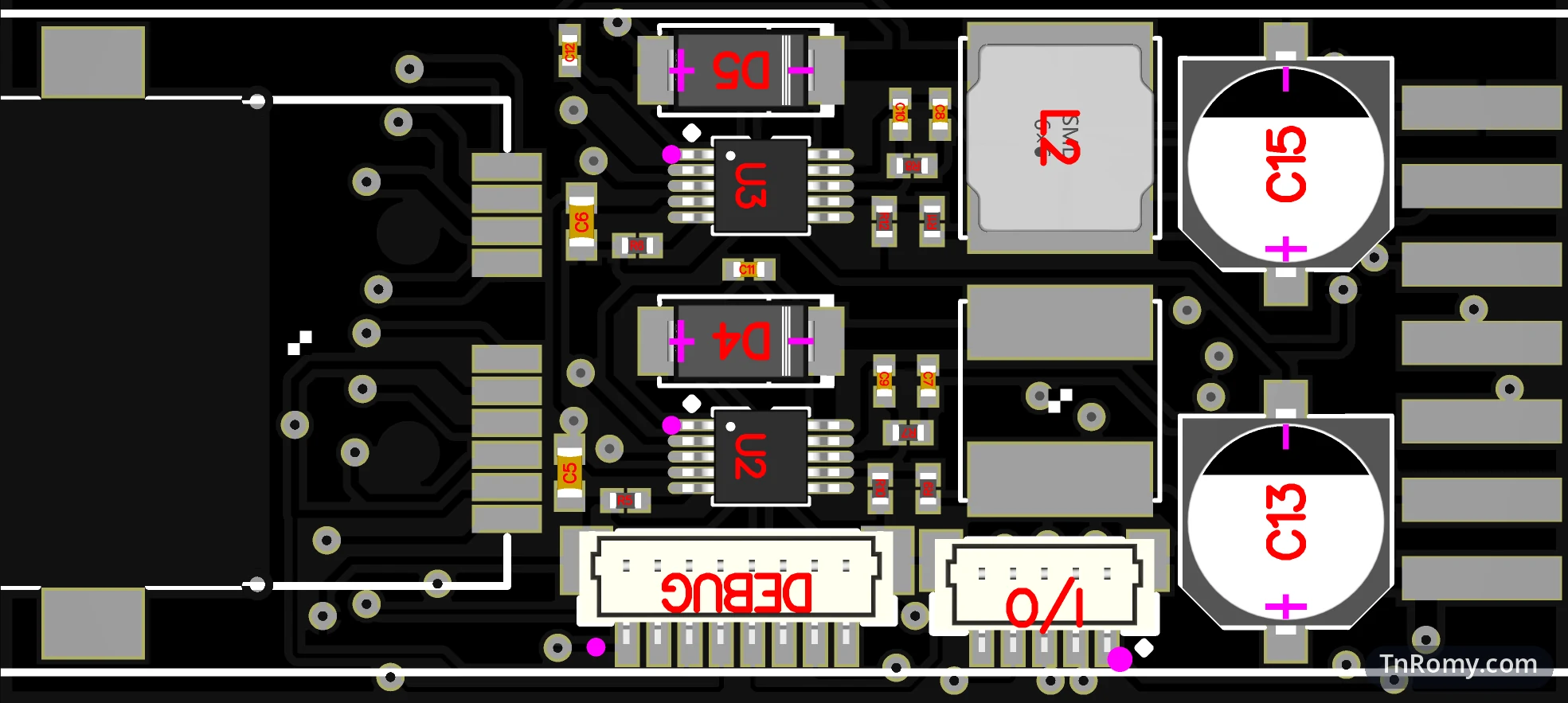
Then the boards arrived and did not power up. A pinout or routing mistake in the PD controller section kept the current from ever reaching the buck converters. I patched the boards with jumper wires to get past that section, and with the wires in place the board runs. That is how v3 ended: a prototype that runs with wires on it, and a lot of material for the next revision.
Design decisions
A microcontroller with Ethernet inside. The CH32V203RBT6 is the cheapest chip I could find with both the Ethernet MAC and the PHY integrated, at around 1.8 USD. The only other candidate I found, the CH32V317WCU6, costs about a dollar more. Because the MAC and a 10 Mbit/s PHY are on the chip, it connects straight to an Ethernet transformer, or directly to an RJ45 that has the magnetics built in. An external Ethernet chip such as the W5500, ENC28J60, or LAN8720 would add to the bill of materials and the assembly cost, it would bring its own set of supporting components, and it would take space that this board does not have. With those constraints, the CH32V203RBT6 was the only logical choice.
A width set by the enclosure rails. The board slides into rails inside an extruded aluminium profile about 25 × 25 mm in cross-section, sold in lengths of 40, 50, 60, 70, and 80 mm. I chose 50 mm, and the board's length follows it. The width is close to that of a common STM32 module, and it is set by the rails.
A sunken RJ45, centred on the cap. The connector sits 2.45 mm down in a slot cut into the board's edge, so the port lands in the middle of the end cap instead of standing proud above it. It keeps the whole enclosure low and symmetric.
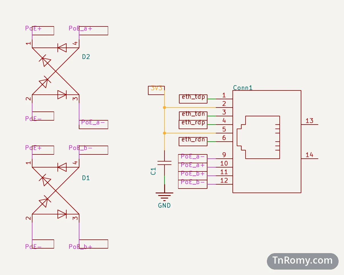
Both PoE modes, any polarity. A power source can deliver PoE over the data pairs or over the spare pairs, and with either polarity. One diode bridge per pair set accepts all of it, so the board does not care what kind of switch or injector it is plugged into.
Two converters side by side, not in a chain. Both buck converters draw directly from the PoE rail, one producing 24 V and one producing 3.3 V, and they share their enable and soft-start signals, so both rails come up together. Neither rail depends on the other being healthy.
One header that serves many kinds of module. The 7-pin header for the rear module carries 24 V, 3.3 V, ground, and four microcontroller pins, PA4 to PA7. I picked those four because together they can act as an SPI bus, each of them is an ADC input, and two of them can produce PWM. One header therefore serves a digital module, an analog one, or one that drives a load.
Block diagram
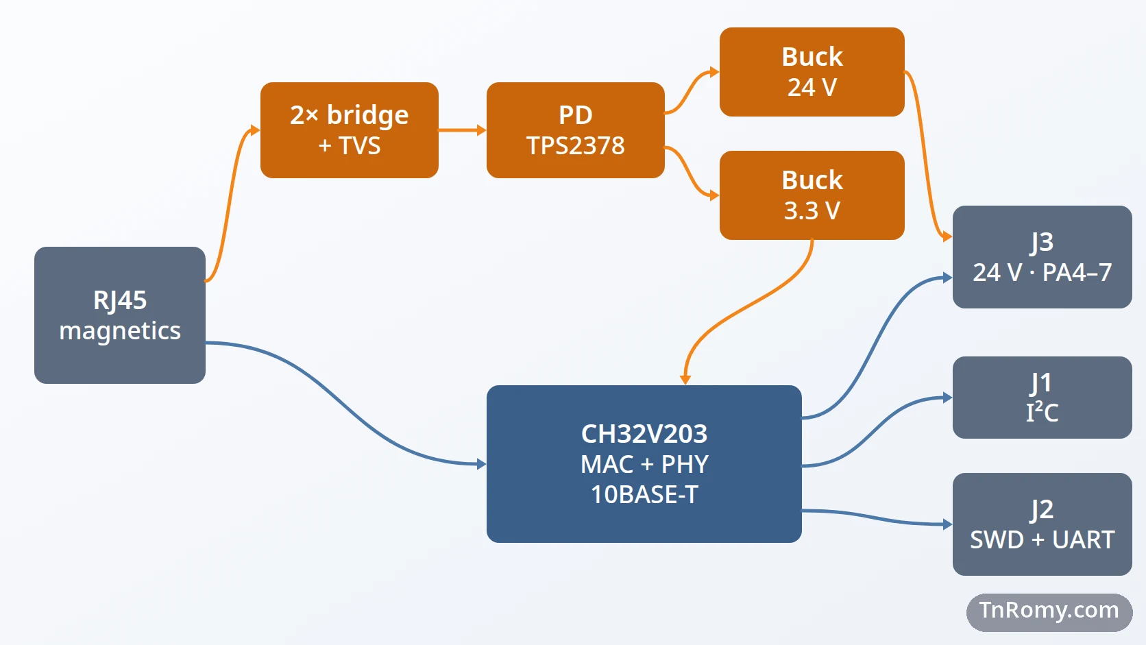
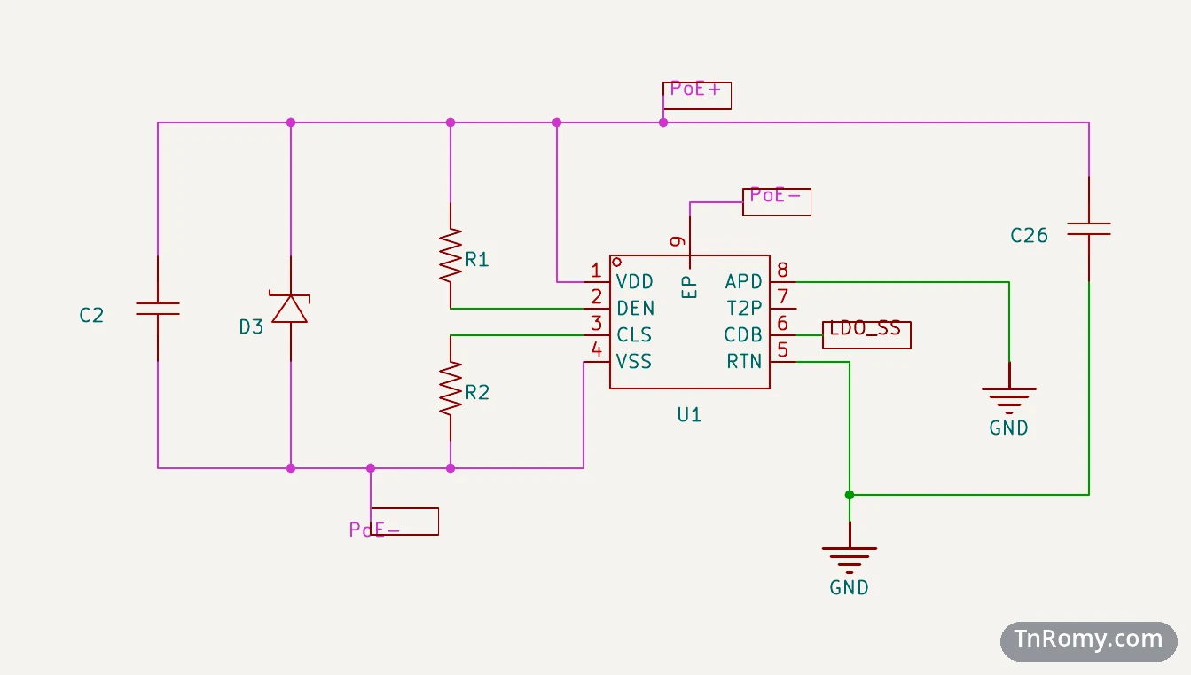
Two pieces of the schematic show the front end in more detail. The values of the parts are left out on purpose: this page is about how the board is put together, not a recipe for building one.
Power
| Rail | Comes from | Feeds |
|---|---|---|
| PoE (nominal 48 V) | The Ethernet cable, through the diode bridges and the PD controller | Both buck converters |
| 24 V | The first buck converter | The module header, for loads such as a fire alarm line |
| 3.3 V | The second buck converter | The microcontroller, the RJ45's center taps, and every connector |
The design is not isolated: the board's ground is the return of the PD controller. That kept the circuit simple, and it is one of the things v4 changes.
Pinout
| Connector | Type | Pins |
|---|---|---|
| J1 · I/O | JST SH, 1 mm, 5 pins | 3.3 V · SDA (PB11) · SCL (PB10) · BOOT1 · GND |
| J2 · DEBUG | JST SH, 1 mm, 8 pins | TX (PA9) · RX (PA10) · GND · SWCLK · SWDIO · 3.3 V · BOOT0 · not connected |
| J3 · module | Pin header, 2.54 mm, 7 pins | GND · 3.3 V · PA4 · PA5 · PA6 · PA7 · 24 V |
The firmware is the same Embassy-Rust firmware I measured in the paper Where the SRAM Goes. For the paper it ran on WCH's official evaluation board, but it runs on all three PoE32 revisions as well, since they share the chip; only the GPIO configuration had to be adjusted for each board. The serial output on J2 is how I follow it during development.
Mechanics
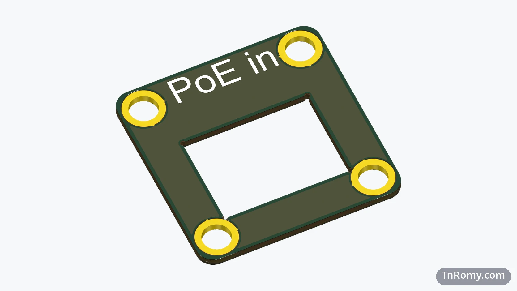
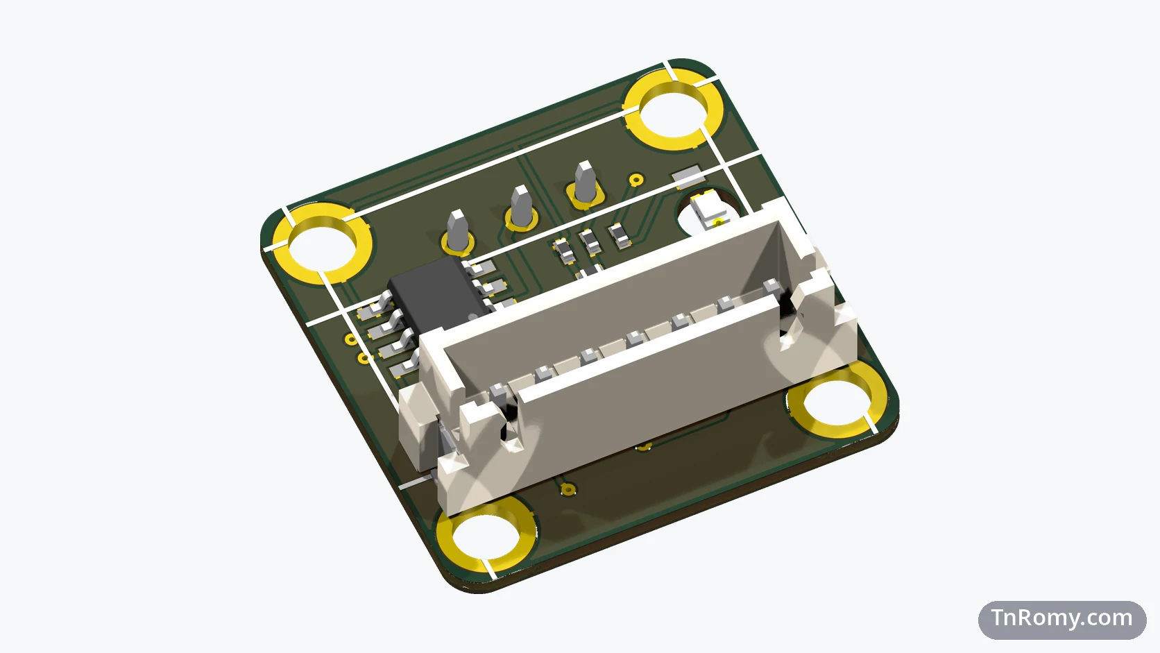
The board is 50.0 × 23.0 mm. The RJ45 slot is cut open to the left edge, 8.2 × 15.5 mm, with two tiny relief drills in its inside corners. The enclosure is an extruded aluminium profile about 25 × 25 mm in cross-section and 50 mm long; its end caps are PCBs of 24.9 × 24.9 mm with the same four bolt holes, one at each end of the profile.
What it taught me
Check power ICs against the datasheet, symbol and footprint both. Pin numbers, the exposed pad, and pins with more than one function have to be checked against the datasheet before ordering, above all when the symbol came from someone else's library.
Leave a way in. Test points and footprints for 0 Ω resistors along the power path would have let me isolate the fault on the board instead of patching around it with wires. Every power path on the next revision gets them.
Isolation is worth its space. A non-isolated design is simpler, but it makes measurements awkward and it does not provide the isolation that the 802.3 standard expects.
Those three lessons shape v4. It moves to a more integrated PD controller and away from the TPS family, with an isolated flyback converter from 48 V down to 24 V and a buck converter from 24 V to 3.3 V. The board narrows from 23 mm to 22.86 mm (0.9 in): at 23 mm it fits the enclosure rails too tightly, it is hard to slide in, and it could bend when the aluminium expands, while 22.86 mm leaves a small gap. The end caps stay as they are. v1 to v3 were all drawn in Altium Designer on Windows; v4 is being drawn in KiCad on Ubuntu.
None of the three revisions has been installed anywhere yet. They were not finished, and v3 still has the defect above. PoE32 goes into real use with v4.
Related
The tool I read the board's serial output with while developing it.
Terms
- Power over Ethernet (PoE)
- Delivering power over the same Ethernet cable that carries the data.
- Powered device (PD)
- The side of a PoE link that receives power, such as this board.
- Power sourcing equipment (PSE)
- The side that supplies power, such as a PoE switch or injector.
- Mode A and Mode B
- The two ways a power source can deliver PoE: over the data pairs, or over the spare pairs of the cable.
- MAC and PHY
- The two halves of an Ethernet interface: the MAC handles frames, and the PHY turns them into signals on the cable.
- Magnetics
- The small transformers between an Ethernet chip and the cable, which some RJ45 connectors have built in.
- Buck converter
- A switching regulator that steps a voltage down efficiently.
- Flyback converter
- A switching regulator built around a transformer, which can keep its output isolated from its input.
Technologies covered
- Altium Designer
- CH32V203
- Microcontrollers
- PCB Design
- RISC-V
- Ethernet
- Power over Ethernet
Attachments
-
Download
PoE32-v3.step (zip)
3D model of PoE32 v3 with components, STEP format
5.3 MB